2900 Lab
Lab Section 2
Group 3
Asmus, John
Chan, Beckie
Chen, Michael
Chiu, Michael
Thammasatit, Peter
Introduction
The objective of this project was to create an AM2900 microprocessor using our previously built AM2901 alu and AM2910 sequencer. This processor is used to implement a binary coded decimal converter.
The binary coded decimal program is written in assembly language. We had access to twelve different macroinstructions: STM, ADD, SUB, OR, AND, JMP, HALT, LODM, LODI, MOV, JGE, and CMP. After creating this program, it was then parsed and converted to its binary equivalent. This binary file was next stored in a RAM and the ALU2900 implements the instructions.
Each of the macroinstructions is made up of one or
more microinstructions. The function of
the AM2900 is to fetch each macroinstruction, find its corresponding
microinstructions, and implement the microinstructions. The following is a summary of some of the
major components of the AM2900. One of
the essential parts of the processor is the instruction register. This register obtains macroinstructions from
the outside RAM, which are latched in whenever WR_EN is enabled. The Mapping PROM takes the four bit opcodes
of the macroinstructions and finds the address of its corresponding
microinstructions. This address is then
passed to the sequencer which controls the flow of microinstructions to be
implemented. The microinstruction address
is then passed to the microprogram memory.
This logic block generates all the signals necessary to complete the
particular microinstruction. The
signals are held in the pipeline register for one clock cycle before going to
the AM2901. Also before going to the
alu, the macro and micro register decoder adds one bit to the most significant
bit of A and B depending on whether they use macro or micro registers. The alu takes all these signals and
generates a result. Then another
microinstruction or macroinstruction is executed depending on the sequencer.
2900
Architecture
Functionality
and How It Works
Mapping
PROM
The mapping PROM takes the four-bit opcode of the macroinstruction and converts it to the address of the microinstruction. This component was created using a ROM with input of four bits and output of twelve bits.
The following table specifies what
opcode mapped to what instruction. The
opcode is in binary, and microinstruction address is in decimal:
|
Marcroinstruction |
Opcode |
Microinstruction
Address |
|
LODM |
0000 |
2 |
|
LODI |
0001 |
4 |
|
MOV |
0010 |
5 |
|
CMP |
0011 |
6 |
|
JGE |
0100 |
7 |
|
STM |
0101 |
9 |
|
ADD |
0110 |
11 |
|
SUB |
0111 |
12 |
|
OR |
1000 |
13 |
|
AND |
1001 |
14 |
|
JMP |
1010 |
15 |
|
HLT |
1111 |
16 |
All
other opcodes not specified in the table are invalid. So, invalid instructions will map to 0. 0 is the address of the microinstruction, which fetches a new
instruction. The microinstruction
addresses are then inputted to the AM2910 Sequencer. The AM2910 can use this value to find what microinstructions to
implement.
Macro and Micro Register Decoder
The Macro and Micro Register Decoder is simply a multiplexor, which selects addresses from either macro or micro A and B. The RAM of the ALU has a total of 16 register locations, which require 4 bits to address. This RAM is divided in half, allotting 8 locations for macroinstruction storage and 8 locations for microinstruction storage. We made the lower 8 locations for microinstructions and the upper 8 locations for macroinstructions. Hence, in binary, the most significant bit of the micro register locations begins with a 0, and the most significant bit of the macro register locations begins with a 1. The one exception to the division of the RAM is that the macro PC is located at register 0 always.
The 3-bit macro A and B addresses come from the macroinstruction. For most of the macroinstructions, the A and B are found in bits 11 to 6. The 3-bit micro A and B addresses come from the Microprogram Memory. We choose macro or micro A and B depending on the control signal SelMu. SelMu is 0 when macro A and B need to be used (e.g. for instructions LODM, LODI, MOV, CMP, STM, ADD, SUB, OR, AND), and SelMu is 1 when micro A and B need to be used (e.g. for instructions IFETCH, JGE, JMP, RESET). If macro A and B are used, the Macro and Micro Register Decoder places a 1 as the fourth bit of the addresses. If micro A and B are used, the Macro and Micro Register Decoder places a 0 as the fourth bit of the addresses.
After passing through the Macro and Micro Register Decoder, A and B are ready to address the RAM.
The
Extender
The Extender takes the least significant 6 or 8 bits
of a 16-bit instruction and outputs the same number of bits with leading 0’s to
produce a 16-bit number. The purpose of
this is to isolate a value or address variable from the instruction and muxed
it to the 2901X4 ALU.
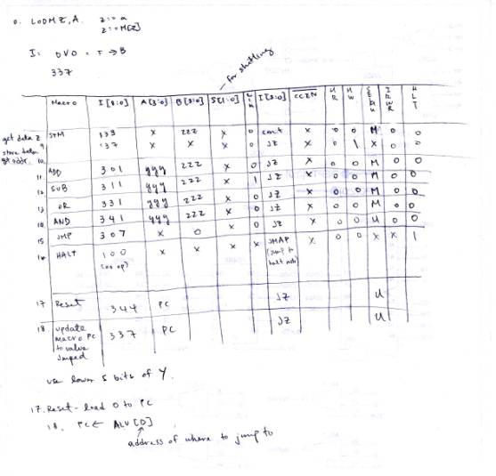
Microprogram
Memory
The microprocessor memory is a list of
microinstructions that execute the different assembly instructions. Each micro instruction consists of 40
bits. These 40 bits control the
hardware signals that are needed to perform a desired macro instruction. In order to execute some of the macro
instructions, multiple micro instructions may need to be called. In this case, it is the job of the mapping
prom to point the assembly instruction to the block where that set of micro
instructions that is located. Once the
microprocessor receives an input from Y[11:0], it the outputs the appropriate
signals for I[8:0], A[2:0], B[2:0], S[1:0], Cin, I[3:0], CCNBar, BA[11:0], MR,
MW, SelMu, IRWR, and HLT. Here is the
complete Micro-program table:
The majority of the work is done by the two
ROM's. The first takes in the signal
OUTIN[4:0] and outputs the appropriate eight-bit instruction, IALU[8:0], which
is then sent to the ALU. The second ROM
also takes in OUTIN[4:0] and outputs the instruction for the sequencer,
ISEQ[3:0]. The rest of the desired
outputs are controlled by AND, OR and buffers.
HBUS
Interface
The HBUS interface is one level above the 2900 chip
(i.e. the 2900 is made into a macro and the HBUS is used with along side the
macro). Our implementation actually
does not use the HBUS for data input (i.e. the host_rd_data pin) because the
external memory contains the instructions to execute. But to display data on screen, data is sent from the 2900 to the
HBUS (i.e. the host_wr_data pin).
The timing of the HBUS interface and the various
components is a bit tricky. Since our
chip runs only at 1 MHz and the HBUS runs at 33 MHz (PCI bus speed), the clock
needed to slow down for our slow chip.
Thus, we used two toggle flip-flops in series to slow the clock by a
factor of four. Each toggle flip-flop
works by looking at the toggle input: if the toggle input is 1, the flip-flop
outputs Qbar, and Q otherwise. The
output of the toggle flip-flop is sent through a BUFGS module, which is a
buffer connected to a high-speed copper wire (tied to the same copper wire as
the clock). The BUFGS allowed us to
drive a new clock input, whose one cycle is the equivalent of four clock cycles
(of the original clock). That is, the
new clock remains high for four clock cycles and low for four clock cycles.
The same slow down technique is used for the RESET
signal (LAB6 pin in our design). We
placed four flip-flops one after the other.
This causes the reset signal to stay on for four clock cycles.
Pipeline
Register and Overall Timing
The pipeline register module consists of several
flip flops. This allows the chip to
operate as a pipeline; that is, components or sections of the chip can operate
independently of one another. For
example, the 2901 can execute the current instruction while the 2910 processes
the next instruction to execute.
The overall timing of the project with the pipeline
is as follows (note: this was vital information for debugging):
1st
clock cycle
when the first instruction executes, everything
starts at random values.
the RESET signal sets the microprogram memory alu
instruction (i[8:0]) to 344 and the sequencer
instruction (i[3:0]) to 0000.
the microprogram memory value is written to the
pipeline register.
2nd
clock cycle
the mu decoder will select the micro instruction registers.
the 2901 will execute 344 which stores 0 into the
RAM and outputs the 0 result, which is written to the
instruction register. this sets the macroPC to 0.
the RESET signal goes low.
the microprogram memory will execute 104 for the alu
instr. and E or CONT for the sequencer (2910).
the microprogram memory value is written to the
pipeline register.
the sequencer will execute 0000, or the first
instruction loaded from memory.
3rd
clock cycle
the sequencer increments its micro PC to 1 after
executing E or CONT.
the microprogram memory outputs 204 and 2 or JMAP
and the pipeline register stores the values.
the alu executes 104 and increments the macroPC.
4th
clock cycle
the alu executes 204, storing 63 into B = 7, and
outputs the result.
the sequencer executes 2 or JMAP, moving to the LODM
micro instr. block.
the microprogram memory writes 337 and E to the
pipeline register.
5th
clock cycle
the alu executes 337.
the sequencer does a CONT or E.
the microprogram memory writes 237 and JZ or 0 to
the pipeline register.
6th
clock cycle
the alu executes 237.
the sequencer does JZ or 0 to begin fetching the
next instruction.
and the microprogram memory writes 344 and 0000
again to the pipeline register.
the cycle continues in this fashion.
Programming
Parser
The
parser translates MACRO instructions, read from a file, to their corresponding
binary representations (or machine code).
This is done by first reading the input file, and by storing the
macroinstructions and operands into variables.
Each variable is compared with the list of possible MACRO
instructions. If there is a match, the
binary representation is constructed by setting the opcode, destination and
source registers (if any), and the address bits (again, if any). The binary string is padded with zeroes if
no values exist. The binary string is
then written to a file, used for the external memory of the 2900 chip.
Linker
The linker was not necessarily required for full and
correct operation of the parser; but because labels and constants are inevitably
used, the linker allowed the programmer more flexibility and ease when writing
the assembly code. The linker is
executed before the parser is, and it generates a file without labels and all
the defined values translated. The
parser then has a simple task of translating commands into machine code. The linker provides three important
functions, it allows the use of location labels, it allows the use of constant
definitions, and it allows specification of memory locations. Most of these functions are provided through
a preprocessor directive similar to the CUSP (introduced in CS33) preprocessor
directive of “.EQU”.
The linker takes in .EQU commands and operates on
them just like CUSP, the command “.EQU @, loc”
will set the program counter to the number specified by loc. The command “.EQU cName, cValue” will set some constant name cName to the
number cValue; this is similar to the C++ preprocessor directive “#define cName
cValue”. The linker simply searches for
cName in the link list that represents the symbol table, and when it is found
and cValue is undefined, it defines cValue.
Otherwise the linker will create a new symbol cName and associate cValue
to it. Of course the linker does all
the necessary error checking to ensure that there are no duplicate cName
entries, and such.
The linker also takes in labels preceding a
colon. These labels will cause the
linker to search the symbol table to ensure no duplicates names, and then
associate the program counter with the label.
All these routines are done with the first pass of the linker.
The linker also translates symbols that are already
defined in the table to the corresponding value in the first pass. Unfortunately, some symbols maybe used
before they are defined, such as jumps to exit a loop. For these symbols, they are processed during
the second pass, which links all the symbols completely. Once this is done and output into a file,
the job is then handed to the parser, which will finish the compilation
procedure.
Assembly Program
The AM2900 processor was used to implement an assembly program which converts a 16 bit number into binary coded decimal. This 16 bit number is represented in decimal in our assembly program because all instructions are supposed to be given in decimal. The largest decimal number the processor can take is 9999. For macroinstructions, we were allowed to use 8 registers only.
Our assembly program begins with ".EQU @, 0." This line specifies that the first instruction begins at address 0. We also use the ".EQU @, N" where N is an address, followed by "DATA" to directly store constants into memory. For example, we placed the number to be converted in RAM at location 63.
To begin the program, we loaded the number to be converted from memory, M[63], and stored it into register 7. We used register 0 as the counter and initialized it to 0.
Then, we had to calculate how many 1000's were in the number. This was done by subtracting 1000 from register 7 and incrementing the counter until the number was less than 1000. The counter value then had the number of 1000's in our input. For instance, if the input was 3245, then the counter would increment to 3. This was then stored in register 6.
Next, we found how many 100's were in the number in a similar fashion. Counter was set to 0 and we subtracted 100 from the modified input until it was less than 100. The counter value was then stored to register 5.
Same was done to find how many 10's were in register 7. This value was stored in register 4.
Finally, we were able to start converting the input into BCD. The number which now remained in register 7 after subtracting 1000's, 100's, and 10's, is only the 1's digit. This value is already in the hex form of the BCD for the 1's place.
To obtain the hex form of the BCD for the 1000's place, we multiply register 6 by 4096 and add it to register 7. 4096 is 0001 | 0000 | 0000 | 0000 in binary. Therefore, if we multiply it by register 6, we will obtain the BCD of the 1000's place digit in the correct location.
To obtain the hex form of the BCD for the 100's place, we multiply register 5 by 256 and add it to register 7. 256 is 0000 | 0001 | 0000 | 0000 in binary.
To obtain the hex form of the BCD for the 10's place, we multiply register 4 by 16 and add it to register 7. 16 is 0000 | 0000 | 0001 | 0000 in binary.
Our final result of the input converted to BCD is in register 7. We then store this back into memory at address 63.
HLT ends the program.
Simulation
Results
The worst path delay was generated from the cinout
coming from the pipeline register. This
path ended at the Data_B3 of the register that stores the uPC+1 inside the
sequencer. This path has a delay of
509.879 ns which results in a minimum period of 1019.758 ns. This means that our system can operate at a
maximum frequency of 0.981 MHz.
The number of Configurable Logic Blocks that were
used for this processor is 362 out of the 1024 available. The equivalent gate count for third design
is 15097 gates. The processor simulated
correctly and all the results works.
Conclusion
for the 2900
Did
it work? What did not? What could be done better?
The 2900 CPU worked as expected. We were able to combine the 2901X4 ALU and
the 2910 Sequencer with the HBUS, Microprogram Memory, Mapping Prom, and
various parts to create a limited functional CPU. A parser and a linker enabled us to use the 2900 to convert a
Hexadecimal number into a Binary Coded Decimal number.
After our initial design we came upon certain
problems that we later fixed. The
LogiBLOX mem files used two radix values, one for the “Header” section and one
for the “Data” section. This became
confusing, but we simply had to check that the radix values were correct for
our data.
The JGE had to be modified to jump when N = 0, and a
different set of microinstructions had to be executed on this case. To solve this, a MUX was used to select
either the current instruction or the microinstruction block to handle a jump
condition.
The CMP macroinstruction needed to have its carry-in
enabled; this is because the CMP function performs subtraction.
Our parser was modified as our LODM was translated
incorrectly in the hardware; we solved the LODM problem by zeroing the most
significant two bits of IR[7:0] (from the instruction register) with the 16-bit
zero extender.
The Microprogram Memory needed to be tweaked several
times, on one case, to adjust the intake of variable bits for different
instructions.
For the HBUS to work correctly, a modification was
made to ensure the clock would be at a reasonable speed for the CPU, as
explained in the HBUS implementation. A
flip-flop was used in a way to ensure that the output would be sent out 1 cycle
after the HALT instruction is executed.
Two other problems we faced earlier were 1) during HBUS execution, the
2900 chip will run if given clock cycles.
Then, the 2900 will execute random data values and instructions. To prevent this, an ONLINE signal ensured
that the 2900 chip would run only after the RESET signal went high. The second problem was that the DONE signal
was constantly high after the 2900 finished executing. This caused the system to crash the FPGA to
lock. We solved the problem with logic
gates, tying the done to the ONLINE and RD_X signals.
An attempt was made to provide additional access for
a user level way of inputting and outputting the register data using an OUTZ
instruction, but there was insufficient time to do so.
Division of Labor
About five weeks were spent on this project. Normally, class sessions are two hours long, but most of the time, the team stayed at least an hour longer to work. Sometimes it would be two hours longer and sometimes three. So an average of 2 + 1.5 hours per class session and 15 class sessions (three per week) add up to 52.5 hours. Six of these hours were spent on the original design phase while programming a parser and the assembly code took up about two hours. The next 21 hours were needed to make the HBUS work. During those 21 hours, we encountered name conflicts and strange implementation errors. Thus, we wound up changing the name of the design from 2900 to A2900 to am2900 and finally to lab6. The name ‘lab6’ worked and Xilinx implemented the HBUS properly.
But the HBUS and the 2900 chip did not function correctly. About 23 hours were needed to fully debug the system. Several hours were spent looking at simulation results to see if the correct values were being output, and which instructions were executing at each clock cycle. By doing this, we noticed several errors including instruction and design errors. More hours were used to fix the HBUS by slowing the clock to the 2900 chip’s speed.
In addition to the extra hours put into class, some team members spent time outside of class to work on the project. Michael Chen spent about 30 hours, 16 hours outside and about 10 hours at home. He has accounted for his hours as follows:
2 hours to finish the design.
7 hours for coding the linker and parser program
15 hours in debug phase analyze the simulation files,
2 more hours to tidy it up. make a binary displayer, nicifying the interface.
4 hours for the report.
Beckie Chan spent 6 hours outside of the lab for debugging and 3 hours for the lab report. She missed one class session.
Peter Thammasatit spent 3 hours on the report.
John Asmus spent 2 hours on the report and missed 3 class sessions.
Michael Chiu spent 5 hours on debugging, 4 hours on writing the parser, and 4 hours on the report. He missed one class session.