Michael Chen
Prelab – Series-Parallel Multiplier
We began the series-parallel multiplier by following the algorithm provided in the directions. First, in state zero, the D flip-flop, register P, and the done signal are cleared. Registers A and B are loaded with their values. Next, when the user inputs run = 1, state 1 is executed: the least significant bit of A is multiplied with B and stored into P. If run is still equal to 1, it will move on to state 2 where both the D flip flop, P register and A register are logically shifted right. Next, it goes back to state 1 and everything is repeated three more times. Once all the bits of A are multiplied with B, the done signal goes high. If the done is high and the run is still equal to one, the system will just hold the final product. Once the run becomes low, it goes back to state zero.
A table was made to find the controls needed to shift and load the A, P, and B registers.
Design and Implementation
We started our design with the three shift registrars (74194 chips). These registrars are used for A, P, and B. Also, a D flip-flop is used to shift into the P registrar the carry output of the full adder. The outputs from the B registrar are connected to a mux whose select depends on the last bit of A. When the least significant bit of A = 1, the B value is passed to the full adder. When this bit A = 0, the value zero is passed to the full adder. This is equivalent to multiplying the last bit of A to B. On the other input of the full adder is P. Once added, the sum is stored back into P. The carry out of the full adder is saved into the D flip-flop. Next, a shift right occurs. The value stored in the D flip-flop shifts into the P registrar, and the least significant value of P is shifted into the A registrar. This whole process is done again three more times.
Clearing registrars, loading bits, shifting bits, and setting the done flag are taken care of by spcon. This system was created using a tdf file because it was more convenient than using a graphical editor. The DoneSet output sets the Done signal to one when the counter equals 7. Since there are eight steps in the algorithm, we know that the final product must be present in A and P once the clock reaches 7. DoneClr clears the Done signal once Run is set to zero again. The S1, S0 values of the registrars depended on the state, on Run, and on Finish. If Run ever equaled zero, the system would go directly to state zero. Also in state zero, the P registrar had to be cleared and A and B had to be loaded. So the PClrn is set to 0 to clear P at state zero. The BMS0, BMS1 = 1, 1 at state zero to load new values. Similar settings were done for AMS0 and AMS1. In order to shift right at state two, AMS0 and AMS1 are set to 0, 1 at this state. Also, PMS0 and PMS1 are set to 0,1 in order to shift at state two. The output of the D flip-flop is placed at SRSl of the P register in order to shift in the carry out bit.
A special state 3 was added in case the user tried to continue multiplying (leaving Run = 1) after the product was already computed (Done = 1). In this case, the system will hold the product and continue holding until Run is cleared. Once Run = 0, the system goes back to state 0.
Observations
One of the main problems we had involved the order of the bits. When loading the bits into the registrars, the most significant bit went into input A. We followed this convention when loading these bits into the adder (most significant bit going into input A). However, we discovered that our results from the adder were incorrect. This error occurred because we input the bits in the wrong order. For the full adder, the least significant bit goes into input A. After switching the lines around, we finally obtained correct results from the adder.
Another problem we encountered was that the multiplier would stop too early. Our done flag was only based on the counter. However, we discovered that our counter would reach seven before the bits finished multiplying because the counter started too early. We needed to reset the counter after state zero. We tried to reset at state one, but it would reset four times for each calculation which is not what we desired. Therefore, to delay the done flag, we tried adding a series of not gates. This proved ineffective because the propagation delay of a not gate is very short. However, adding a D flip-flop into the system solved the problem. This saved the result from the previous cycle and outputted the value in the next cycle. This allowed the multiplier to finish multiplying before the done flag went high.
PreLab:
B3 B2 B1 B0
C2 C1 C1
C2 C1 A0B3 A0B2 A0B1 A0B0
C2 C1 A1B3 A1B2 A1B1 A1B0
C2 C1 A2B3 A2B2 A2B1 A2B0
OUT8 OUT7 OUT6 OUT5 OUT4 OUT3 OUT2 OUT1 OUT0
Design/Implementation:
In order to implement a parallel
multiplier, we first needed to know what the output bits came from. So we algebraically multiplied two four-bit
numbers and concluded that the output was the sum of certain bits. We also noticed that we encountered need to
add four bits at a time, and we found that two carries were possible.
In order to accomplish this
operation we set forth to design a four-bit adder with two carry in. When all six inputs, the four bits and two
carries are one, then we needed to output six which is 110 in binary. This meant we had a second order carry out
affecting results of the add two bits higher, a first order carry out affecting
only the add in the next column, and a result in the current column. In making the fulladd4 unit, we saw that a
full adder can add two bits and one carry; and we needed twice as many carries
and bits. So we used two full adders to
obtain the result. The results of the
two full adders were then summed which generated out result for this
column. A carry was also generated by
this second level operation. We noticed
that carries of the three adders we had so far represented bits of the next
column, so we added all three with another full adder. This full adder generated a first order
carry as the result, with a second order carry on the carry bit. We also decided it would be easier to leave
unused bits unwired, so we made certain the default valued for unwired inputs
were set to ground.
We also needed a full adder and we had designed one for the previous one so we just simply use that one. Which we designed by using a table, and determined all the possible outputs for the sum and carry out given inputs A, B, and a carry in. Our resulting expressions were minimized using boolean algebra.
Once we had these two adder units to work with, we started to make our parallel multiplier. The first thing we did was draw out our input lines and ANDed them together for the correct terms to be added. Then we piped the corresponding terms to the adders and the outputs were tied to our output. We also tied all the carry outs to the carry ins of the next adder unless it was a CR1 which was a second order carry. For the CR1 output, we tied that to the carry in the adder after the next.
Observations/Problems
When we finished the
graphical design file, we noticed we had nine bits of output. The largest possible answer with two
four-bit numbers is only eight bits.
This O8 line seemed counter-intuitive, but we kept it in. In further analyzing the circuit we noticed
that the last two fulladd4 did not have all their inputs used. This would make it impossible for either one
to generate both carries. Both of these
adders must generate both carries in order for the carry to propagate all the
way to O8. Since this was impossible O8
would always be 0. And this explained
the warning that we received from the compiler saying that O8 is stuck at
ground.
Another problem came up when
we were simulating the circuit. We
piped in the value F for input A and the value F for input B. This generated a result that did not match
our expectations. After looking it over
we noticed that when expanded the output bits were correct. Then we noticed that our bits in our
groupings were reversed. After fixing
this problem by reversing the bits and running a couple of trials through we
noticed that the unit was performing as we designed it to, and that the unit
worked.
We notice that the system
does take a short time where the output fluxes before arriving at a stable
answer. But this time was really,
really small compared to time we keep the input stable. We realize this is the time delay that the
input takes to go through all the combinational logic.
Michael Chen
Design of the serial adder involved multiple steps. We began by designing our own full adder. Using a table, we determined all the possible outputs for the sum and carry out given inputs A, B, and a carry in. Our resulting expressions were minimized using boolean algebra.
Once
the adder was created, we began the main design. Inputs A and B are run through two input muxes. The new inputs are only selected when S1, S0
= 0, 0. Otherwise, on the mux of A, the
old value of A output is read in, and on the mux of B, the output of the full
adder is read in. After passing the
muxes, A and B are serially entered into registers. The most significant bit of A is taken and saved into a D flip
flop. This value is used to determine
whether A is positive or negative.
Further description of the purpose of A's most significant bit are
explained later. After the inputs are
loaded into the register, they are then inputted to the adder.
When
S1, S0 = 0, 1, the function, add, is implemented. This is done by taking the "Q" values from both A and B
registers and inputting them to the full adder bit by bit. First, the carry in value of the adder is
set to zero. Next, each bit is added
together and carry outs are saved for the next addition using a D flip
flop. The carry out becomes the carry
in for the next 2 bit addition. After
each bit addition, the output is saved into register B.
When
S1, S0 = 1, 0, a subtraction is done.
Therefore, A must be complemented before being added to B. A 2's complement is done by reading from the
"NQ" of the A register. Then
A' and B are passed to the full adder and the carry in is set to 1 to complete
the complement of A. Like in the
addition procedure, the carry outs are saved in the D flip flop, and the output
is fed into register B.
When
S1, S0 = 1, 1, the absolute value of A is taken and saved into B. The system checks whether A is a negative
number or a positive number by taking the most significant bit of A. On the eighth clock cycle (when c0, c1, c2 = 1, 1, 1), the A bit is
saved into a D flip flop. If this bit
is a 0, then A is positive, then the "Q" value is taken from the A
register to the full adder. If this bit
is a 1, A is negative and must be complemented by taking the "NQ"
from the register. In both cases, the other
operand of the adder is a 0 because the absolute value only involves A. However, in the case of A is positive the
carry in of the full adder is zero, while in the case of A is negative, the
carry in is set to one. The final
result is sent to the B register.
In
addition to this data path, a controller had to be designed to manage the
selects of the muxes and carry in of the adder. The selects to input A and B into the registers were equal to
zero only when S1 and S0 both equaled zero, otherwise the data on the
"1" input side was chosen.
This is equivalent to an or gate, MA = MB = S1 + S0. Next, the select for the input of the adder
was created. On the A side of the
adder, we wanted the input to be the "Q" of the register for
adding. For subtracting, we wanted the
input of the adder to be the "NQ" of A. And when taking the absolute value, the mux select is equal to
the most significant bit of A. This
resulted in our design for MAO = S0' + S1S0(MSB). MBO selects the "Q" of the B register for adding and
subtracting and selects 0 when taking the absolute value. Therefore, MBO = S1S0. The carry in was set to 1 when subtracting
and when taking the absolute value of a negative number. This resulted in the equation CR = S1'S0 +
S1S0'(c0+c1+c2) + S1S0(MSB)'. The
(c0+c1+c2) term represents the instance of the first clock. This is used because we only want to
generate a carry on the first clock cycle.
We set the adder to not include a carry when the function was set on add
and when taking the absolute value of a positive number. This gave us the equation NCR = S1S0' +
S0S1'(c0+c1+c2) + S1S0(MSB).
Finally,
the last part of the system to implement was the overflow. We found that overflow occurs when adding
two positive numbers and getting a negative number, adding two negative numbers
and getting a positive number, subtracting a negative and positive and getting
a positive, subtracting a positive and negative and getting a negative, and
taking the absolute value and getting a negative number. A table was made for the first four cases,
and the and-or expression was found.
This expression was anded with (c0*c1*c2) so only the most significant
bit of A and B would be used. In the
case of absolute value, we checked the most significant bit of the output to
make sure that it was a 0. If it was a
1, overflow occurred.
Observations/Problems
One problem that we ran into occurred in the control box of our circuit. At first we attempted to simplify all the logic to use the minimal number of gates, but found a difficult process. We realized it was most efficient to leave the terms as the sum of products. Despite this the control box would still not work properly. When we double checked the connections we noticed that the errors came from misconnections due to the high number of wires that crossed over. We had to be careful with the control box once we discovered this source of error. We occasionally ran into this same problem a few more times, but we finally finished a control box we were satisfied with.
Once we completed the
circuit and simulated it we noticed that the counter circuit incremented on the
falling edge of the clock while the rest of our circuit operated on the rising
edge of the clock. At first we allowed
tried to continue with this design, but soon realized that many errors occurred
from this design. Later we implemented
the counter on the inverse of the clock.
So the counter updated at the same time the rest of the circuitry was
updated.
At first our initial carry
bit was placed by either clearing or setting the d flip flop with the clear and
set pins. We noticed that this caused
the d flip flop to ignore the carry result of the least significant bit because
the set or clear pin was still active.
In order to solve this problem we implemented the carry and no carry
bits as half clock signals. So the d
flip flop would only clear or set on the first half of the clock. This technique worked very well in the timing
simulations and we attempted to implement this with the Altera chips.
Now we noticed that the
Altera chips would not perform our circuit as we have designed it. The timing diagrams from the computer
simulations did not agree with the physical results we got on the Altera board. We were very confused by this result and did
not understand why the Chip did not function as the simulation stated it
would. We sought help from the T.A. and
he suggested that the half clock procedure was slightly odd and to eliminate
the need for it by changing our method of implementing our initial carry. So we did as he suggested and used a
multiplexer to feed our system the initial carry, and we eliminated the half
clock circuitry.
The system worked except for
certain cases where the result of the previous operation returned a carry. We noticed that we did not have a way of
inputting an initial carry of 0 in the case of addition. We realized that a 2 input multiplexer is
not sufficient for our task and we had to use an 8 input multiplexer. So we implanted the system so it would input
an initial carry of 1 for subtract and absolute if the value was negative, and
an initial carry of 0 for add and absolute if the value was positive or 0.
Michael Chen
Design Explanation
Prelab:
We began the design by completing the inputs of the D flip-flops shown in the Prelab. For a load, the inputs of the D flip-flops are any arbitrary values to be loaded in at the fall of the clock edge. For a count up, a full adder is used to add the previous state with zero and a carry in of 1. The output of the full adder is then inputted into the D flip-flops. We ignore the carry out bit of the full adder, so if the old state is "1111," the new state after count up will be "0000." Rotate right, rotates each bit to the right, taking the least significant bit to the most significant bit. Logical shift right shifts each bit to the right and brings in a "0" to the most significant bit. Logical shift left shifts each bit to the left and brings in a "0" to the least significant bit. Rotate left shifts each bit to the left and brings the most significant bit to the least significant bit. Arithmetic shift right shifts each bit to the right but instead of bringing in a "0," it brings in the number that matches the second to most significant bit. Hold will keep the old values of the D flip-flops.
Implementation:
Once we defined each operation, we decided to use multiplexers to implement the register. Since there are four bits of input, we used four multiplexers. Each mux needs to handle seven different operations, so three select lines are needed for each mux. The output of the muxes are inputted into D flip-flops to hold the results.
Determining the individual inputs for each mux was based on the value of M. We used M as the input for the select lines. For M = 0, we input into the 0 pin of each mux the corresponding input values for a load determined in the prelab. For M = 1, we input into the 1 pin of each mux the corresponding input values for an increment by 1 determined in the prelab. The same procedure was used for M = 2, 3, 4, 5, 6, and 7.
Timing Diagram:
Once the general register was designed, we tested it using a timing diagram. We first loaded "1101" into the flip-flops using M = 0. Then we set M = 2 which rotated the bits right to "1110." Inputting M = 3 caused a logical shift right, so the flip-flops held "0111." Then M = 4 caused a logical shift left: "1110." Rotating left, M = 5, gave an output of "1101." M = 6 resulted in "1110." Finally, M = 7 gave "1111." These results matched our expected results.
Altera 7128 Chip
After confirming the accuracy of our design, we loaded it on the Altera chip. The outputs, Q3, Q2, Q1, and Q0, were connected from the Altera chip to LEDS and the inputs, D3, D2, D1, D0, M2, M1, and M0 were connected from the chip to the switch pins of the Altera board. The clock was set up as in previous labs. A D flip-flop was used to create a clean signal. The clear and reset of the flip-flop were connected to the push button switch, and the output of the flip-flop was the clean clock for the register. The *.rpt file was used to determine where each input and output should be connected to the Altera 7128 chip.
Observations
Overall, this was a very successful lab. We were able to design and implement the general register with little difficulty or debugging. The only problem encountered occurred while setting up the D flip-flop to create a clean clock signal. All inputs and outputs were set correctly, but the clock did not give a signal when the push button was pressed. We later discovered that the 7474 chip used was defective and immediately replaced it with a working one. Once the new chip was in place, everything was functional.
Michael Chen
.
Observations
Part 1
The debounce module can be inserted in our GDF design file to supply us with a clean signal. The module will count down from 255 when the input signal is high. The module will restart counting at 255 every time a low signal is detected. So this module will output a signal when input remains stable for 255 clock ticks. So we can connect any unclean input to this module and the output of this module can supply our circuit with clean input signals. This module uses a clock, if the onboard clock is used, the module is useless because the onboard clock runs at 25 MHz. Even 255 clock ticks is still less than a millisecond at 25 MHz. In order to bypass that we would need to pipe in an external clock. We would definitely need to modify the circuit so it counts down from a smaller number (pressing a button 255 times is not feasible). To decrease the counter amount, we just use less flip flops; change count_reg from a 8 flip flop register to a 3 flip flop register.
We can take a 7474 D flip flop and create a clean clock signal controlled by a push button. We connect the reset (pin 1) to the normally close pin on the push button. Clear (pin 4) would be connected to the normally open pin on the push button. And the button is connected to ground. This would allow us to generate clean clock edges.
Part 2
In this part we are supposed to use 74XX
chips to implement a pattern detector that will output a 1 whenever an even
number of 0’s followed by two 1’s followed by an odd number of 0’s is
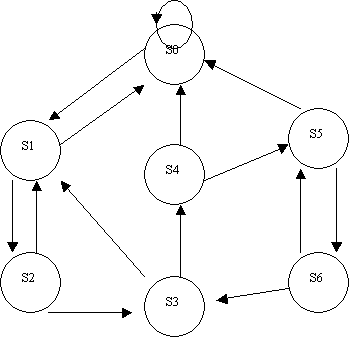
encountered. We implemented the
following state machine given to us by the handout.
Problems Encountered:
The first problem that we encountered was
that the switches provided a low signal when it was closed. This means that the x input was a 0 when we
closed the switch and a 1 when the switch was open. There was two ways to solve this problem, one way is to pass the
input x through a not gate which would then reverse the values. Another way was to say closed means 0
arbitrarily, and opened means 1. In
this part II we solved this problem by wiring the x input through a not gate.
The second problem was a loose connection in
our circuit which did not allow any of our signals to travel from one gate to
another.
The third problem which caused the most
problems was the first 7410 3 input NAND chip we used was bad. Pin 11, which is specified to be C3 input,
was feeding a high voltage into our system.
C3 was connected to Y0’ in effect, it was like Y0’ was hard wired high
all the time. After we changed the 7410
NAND chip, the circuit worked perfectly.
Part 3
In this part we are assigned to implement the
same pattern detector using the Altera MAX EPM77128 chip. After creating the GDF file, we tested it
with a simulation. After programming
the chip with our circuit, we proceeded to wire the chip to the appropriate
input and output signals based on the .rpt file.
Problems Encountered:
The first problem was to
avoid using the internal 25 MHz clock for the flip flops. This was done by passing the clock input
through an and gate with a hard wired 1 for the other input.
The second problem was
that the states were changing at both the rise and fall of the clock, and
sometimes they would even change while the button was not released after
pushing. The Altera chip was much more
sensitive to unclean inputs than the 74XX chips. At this point we had already followed the instructions on
creating a clean clock source from a D flip flop, but the problem
persisted. We found out that the chip
was not up to peak performance, and would cause unclean signals. In order to fix this, we had to connect both
the reset and set pins to VCC through resisters. The resister was used to prevent a short from occurring. We connected a 100k ohm resister rated at 5%
for the set and reset. After the
modifications, the set and reset would rise to VCC unless GND was applied to it
specifically. After resolving this
problem, the pattern detector worked perfectly.
|
|
||
|
Home | About Me | Text Depository | Future Enhancements | Guest Book | Links
All Rights Reserved. |